This repository provides a minimal physical reference PCB
that anchors abstract control and logic concepts into real voltage, current, and copper.
It is intentionally small, generic, and architecture-agnostic,
focusing on observability, physical constraints, and manufacturability rather than functionality.
| Language | GitHub Pages 🌐 | GitHub 💻 |
|---|---|---|
| 🇺🇸 English |
The purpose of this board is not control, but grounding.
- 🔌 Fix abstract logic into measurable V–I behavior
- 👁 Provide a visible and probe-able physical endpoint
- 🧱 Act as a lowest-level physical reference, reusable across systems
This board can be used by higher-level architectures
(control logic, supervisory layers, AI reasoning),
but it does not depend on them.
This repository contains a reference PCB, not a product.
The board includes only elements required to expose
the relationship between logic and physics:
- 💡 LED — observable output state
- 🧮 Resistor — physical constraint (current limitation)
- 🔘 Switch — discrete physical event input
- 📍 Test Point — voltage / current measurement access
- 📐 Board outline (Edge.Cuts) — explicit physical boundary
Nothing more.
All schematics, PCB layouts, and 3D views used in this project are normatively indexed and embedded on the following page:
👉 Image Index (v0–v3)
https://samizo-aitl.github.io/aitl-physical-reference/docs/img/
v3 figures are provided for derived control reference boards and do not modify the normative v0–v2 physical reference.
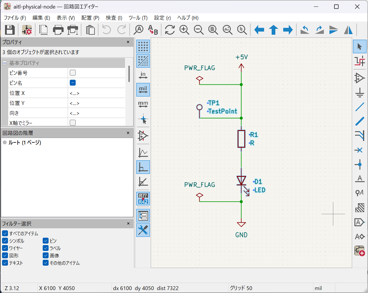
This schematic defines the normative logical–physical boundary:
a logic-driven output constrained by real voltage and current,
with explicit measurement access points.
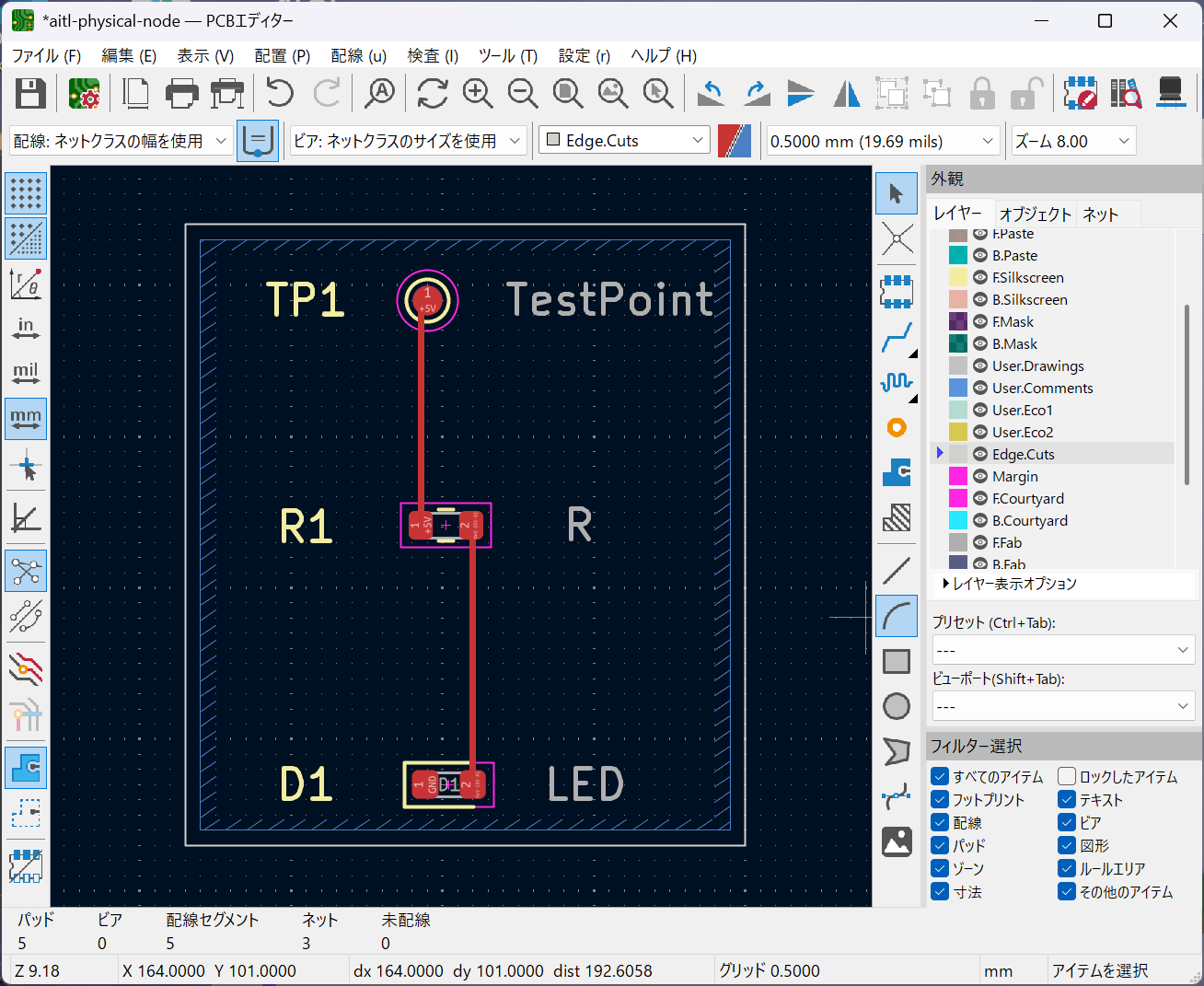
The PCB layout exposes the fixed physical constraints:
- 🟠 Copper routing and current paths
- 📦 Component placement tied to observability
- ⛓ Explicit board boundary (Edge.Cuts)
This layout is the authoritative physical truth for v1.
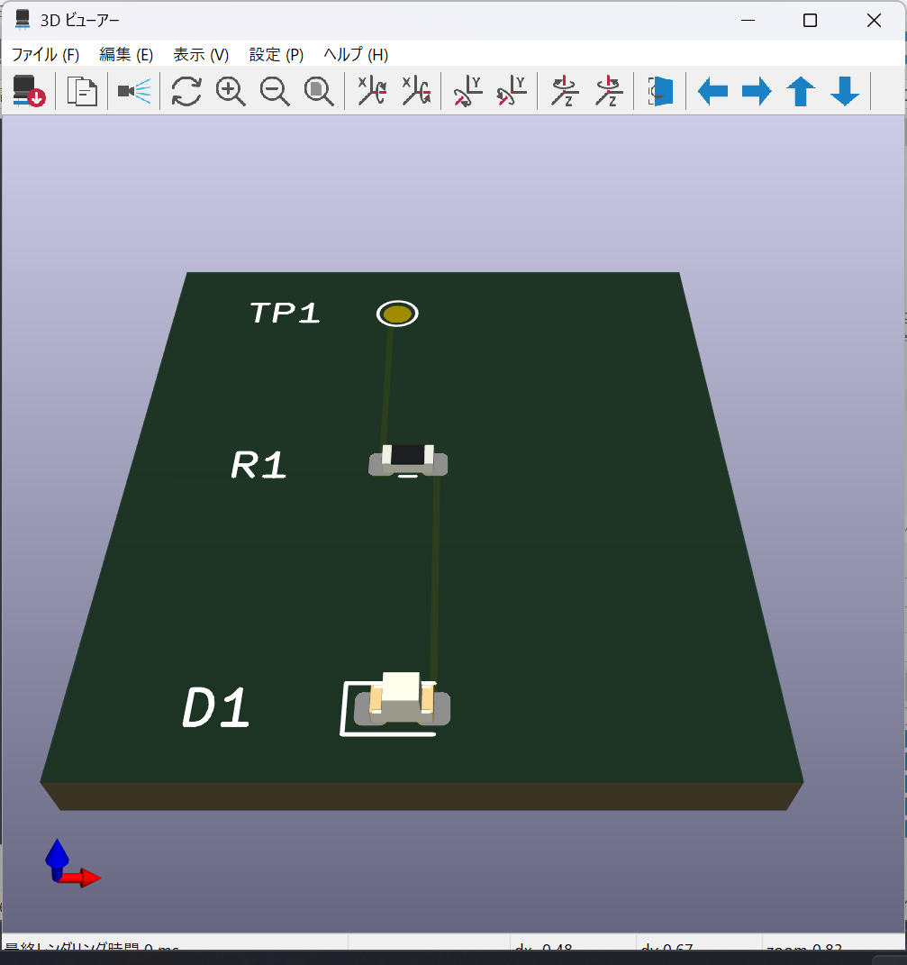
The 3D view represents the embodied boundary between logic and physics:
real height, real clearances, and real probe access —
nothing abstracted, nothing implied.
- ❌ Not a full controller
- ❌ Not MCU-centric
- ❌ Not performance-optimized
- ❌ Not tied to any single architecture or framework
- ❌ Not a demo board for features
This repository intentionally avoids solutions and focuses on reference.
| Conceptual Role | Physical Element |
|---|---|
| Output state | 💡 LED |
| Constraint | 🧮 Resistor |
| Event input | 🔘 Switch |
| Observation | 📍 Test point |
| Boundary | 📐 PCB outline |
This mapping is the core value of the project.
aitl-physical-reference/
├─ hardware/
│ └─ kicad/ # KiCad project (schematic / PCB)
├─ bom/
│ └─ bom.csv # Component list (non-CAD)
├─ docs/
│ ├─ Assembly.md # Assembly instructions
│ ├─ TestProcedure.md # Measurement & verification
│ └─ DesignIntent.md # Physical design intent
└─ README.md
-
Design Intent
GitHub Page
Repository -
Assembly Instructions
GitHub Page
Repository -
Test & Measurement Procedure
GitHub Page
Repository
- BOM (CSV)
GitHub Page
Repository
- KiCad Project (Schematic / PCB)
Repository
To physically build and use this reference board:
- 📄 Review
bom/bom.csvand prepare components - 🏭 Manufacture PCB using KiCad data in
hardware/kicad/ - 🛠 Assemble components following
docs/Assembly.md - ⚡ Apply +5V power and observe LED behavior
- 📊 Verify voltage/current using
docs/TestProcedure.md
This flow is intentionally simple and repeatable.
This board is designed to be measured, not just powered.
Typical checks:
- 💡 LED ON/OFF state
- 📍 Forward voltage at test point
- 🧮 Current limited by resistor
- 📐 Boundary defined by board outline
These checks validate the logic → physics transition.
- 🧩 CAD: KiCad
- 🎨 Design style: Minimal, readable, single-layer preferred
- 📤 Outputs: Standard manufacturable Gerber data
The design favors clarity over density.
This physical reference can be used in:
- 🎛 Control systems
- 🧠 Supervisory logic
- 🎓 Educational hardware
- 🔁 Logic-to-physical architecture studies
- 🤖 AITL-based discussions and validation
It acts as a ground truth layer, not a controller.
- v0 — Minimal physical reference
- 💡 LED
- 🧮 Resistor
- 🔘 Switch
- 📍 Test point
Future revisions may extend observability,
but will preserve minimalism.
v1 extends aitl-physical-reference from a passive grounding board
into a clearly defined physical–logical boundary reference.
This version does not aim to control, compute, or decide.
It exists solely to define where logic ends and physics begins.
- 🔗 Define a clear GPIO ↔ physical boundary
- 📏 Fix measurable voltage–current expectations at that boundary
- 🧭 Provide a stable reference point for higher layers (FSM / PID / AI)
v1 answers one question only:
“When logic toggles a pin, what does that mean in copper, voltage, and current?”
v1 adds a boundary, not intelligence.
Included
- 📍 Explicit logic-level input/output pins
- 💡 Physical load (LED + R) driven through that boundary
- 📊 Documented expected V–I ranges per node
- 🧪 Test points tied to logical meaning
Explicitly excluded
- ❌ No firmware logic
- ❌ No control algorithm
- ❌ No timing guarantees
- ❌ No optimization
| Layer | Responsibility |
|---|---|
| Logical / MCU | State decision, timing, abstraction |
| v1 Boundary | Voltage level, current flow, observability |
| Physical | Light emission, heat, copper limits |
v1 is the line, not the controller.
| Node | Condition | Expected Voltage | Expected Current | Meaning |
|---|---|---|---|---|
| LOGIC_OUT | High | 3.3–5.0 V | < 1 mA | Logic asserts state |
| LED_NODE | ON | 1.8–2.2 V | 5–10 mA | Physical output active |
| VCC | Nominal | 5.0 V ±5% | — | Power reference |
This table is normative in v1.
v1 serves as:
- 🔹 FSM — physical state confirmation point
- 🔹 PID — actuator-side reality reference
- 🔹 LLM / AI — grounding layer to prevent abstraction drift
Higher layers may change.
v1 must not.
Once released:
v1 electrical meaning SHALL NOT change.
Any extension must:
- become v1.x (documentation / measurement only), or
- move to v2 (control-capable reference)
- 🟢 v0 — Passive physical reference (LED / R / SW / TP)
- 🔵 v1 — Logical–physical boundary reference
- 🟣 v2 — Control-capable execution reference (FSM / PID)
GPIO names in v1 are semantic and directional.
They describe what crosses the boundary, not how it is implemented.
<ROLE>_<DIRECTION>
- ROLE: logical meaning at the boundary
- DIRECTION: signal direction from logic perspective
| Name | Meaning |
|---|---|
LOGIC_OUT |
Logic asserts a physical state |
LOGIC_IN |
Logic observes a physical condition |
PWR_IN |
External power reference |
GND |
Electrical ground |
_OUT: logic → physical_IN: physical → logic
Example:
LOGIC_OUTmeans
“Logic drives voltage/current into the physical layer.”
- ❌ MCU-specific names (
PA0,GPIO23) - ❌ Functional assumptions (
LED_CTRL,PWM_OUT) - ❌ Timing semantics (
CLK,SYNC)
v1 names must remain architecture-agnostic and timeless.
v2 realizes the v1 physical–logical boundary
as a manufacturable, observable, and DRC-clean physical loop.
While v1 defines what the boundary means,
v2 defines how that meaning exists in copper.
- 🧱 Fix the entire V–I loop as a physical fact
- 👁 Preserve observability at every critical node
- 🏭 Ensure manufacturability (DRC clean, Edge.Cuts defined)
- 🚫 Still no control logic, no firmware, no optimization
v2 answers one question only:
“If we freeze the physical loop itself, what remains controllable?”
Included
- 📐 Explicit board outline (Edge.Cuts)
- 🔁 Single, closed physical current loop
- 📍 Test points that do not disturb the loop
- 🧮 Current-limiting elements as physical constraints
Explicitly excluded
- ❌ No MCU
- ❌ No GPIO semantics
- ❌ No feedback or timing logic
- ❌ No intelligence
| Layer | Role |
|---|---|
| v1 | Normative boundary definition |
| v2 | Executable physical ground truth |
| v3+ | Control, supervision, adaptation |
v2 is the last layer before control begins.
Once released:
The physical loop topology and V–I meaning SHALL NOT change.
Any change must advance to v3.
- 🟢 v0 — Passive physical reference
- 🔵 v1 — Physical ↔ Logical boundary definition
- 🟣 v2 — Executable physical loop reference (DRC clean)
- 🔴 v3 — Control insertion reference (FSM / PID)
v3 is NOT part of the aitl-physical-reference core.
It is a derived hardware reference that inserts minimal control into the frozen physical loop defined by v2.
- v0–v2: normative physical reference (this repository)
- v3: downstream control experiment (separate hardware directory)
The authoritative source for v3 is:
👉 hardware/kicad/aitl-physical-control
👉 See Fig.10–Fig.12 in the Image Index
v0–v2 remain unchanged and normative regardless of v3 evolution.
| 📌 Item | Details |
|---|---|
| Name | Shinichi Samizo |
| Expertise | Semiconductor devices (logic, memory, high-voltage mixed-signal) Thin-film piezo actuators for inkjet systems Printhead productization, BOM management, ISO training |
| GitHub |
| 📌 Item | License | Description |
|---|---|---|
| Source Code | MIT License | Free to use, modify, and redistribute |
| Text Materials | CC BY 4.0 or CC BY-SA 4.0 | Attribution required; share-alike applies for BY-SA |
| Figures & Diagrams | CC BY-NC 4.0 | Non-commercial use only |
| External References | Follow the original license | Cite the original source properly |
Suggestions, improvements, and discussions are welcome via GitHub Discussions.