A short and on point tutorial on how to use an ASIC logic synthesis tool and how to get the best out of it. A step-by-step guide is provided here in README.md and also as a 2-part youtube video: https://youtu.be/zlmzODnLIM8 and https://youtu.be/bbl5MgOT6vo
There is also a set of questions available in QUESTIONS.md. A reference script is provided in genus.tcl.
The tutorial is built around Cadence Genus version 21. Most of the commands are identical in previous and newer versions too, so it shouldn't be a problem if you have a different but relatively recent version. The tutorial will use a single design (sha256) and many optimization options will be explored to generate different results. The standard cell library considered in this tutorial is from the ASAP7 PDK. No external downloads are necessary, all design files and library files are already included in this repository. The tutorial is organized in tasks that should be completed in order. Let's get started!
As you follow along this tutorial, in many places you will be asked to write down your results. You can use a table/spreadsheet for that. The following table is a suggestion, where each design we try is a new row. Feel free to give the designs some meaningful names:
| Design | Cell count | Total Area | Slack | Static pwr | Total pwr |
|---|---|---|---|---|---|
| First | 1234 | ... | |||
| Baseline | 1200 | ... | |||
| Clock gating | 1333 | ... | |||
| Target 900ps | 1300 | ... | |||
| ... | ... | ... | |||
| ... | ... | ... |
A script for configuring the path to Genus on CMU servers is provided. The script is called genus.sh and it has to be sourced once for every session/terminal that you open. To source it, type source genus.sh
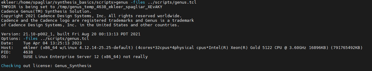
Make sure you can start Genus. If your setup is right, typing genus on a terminal will start the tool. To exit the tool, type exit or press CTRL+C twice. If the installation is correct, you will see something like this on the screen:
It is also important to make sure you have access to Genus documentation. Inside the Genus terminal, type cdnshelp. If your setup is properly installed, a new window will open with Cadence's help navigation system. It looks like this:

On the top part of the window there is a search box. You can use it to find specific commands or terms. For instance, try searching for the word "clock". It will give you thousands of hits. You can search for the command "report_clocks" and then the search results will be much narrower.
Can you find the report_clocks documentation page?
Let's run a reference synthesis script. When using Genus, although the tool provides an interactive shell and a graphical interface, you will almost always prefer to use scripts. To launch Genus and invoke a script at the same time, the syntax is genus -files myfile.tcl.
Genus produces a lot of log files, by default these are stored in the folder where you invoke Genus from. For this reason, it is very common to have a /run folder in your setup. Since you will invoke Genus from the /run folder and the reference script is called genus.tcl, you will have to call genus -files ../scripts/genus.tcl.
This is what the folder structure looks like in this tutorial:
Most of the names are self explanatory. Take some time to browse the folder structure and see what files are there. Do you know what is the purpose of a LEF/LIB/QRC file? LEF files and LIB files are text, you can open them in a text editor and follow the structure. QRC files are binary.
So, did the script start executing? The tool will take about 4 minutes to complete the synthesis run. Do not close the tool just yet, we will collect some results from it in the next task.
We are now going to do some analysis. Typically we are interested in captured timing, power, and area information about a design. We call this PPA, short for Power Performance Area.
First, we will check whether the design is passing timing. The script defines a clock frequency of 1GHz, which is not very aggressive for this 7nm technology. In order to check whether our design is really taking a 1GHz clock into consideration, we issue the command report_clocks. The result looks like this:
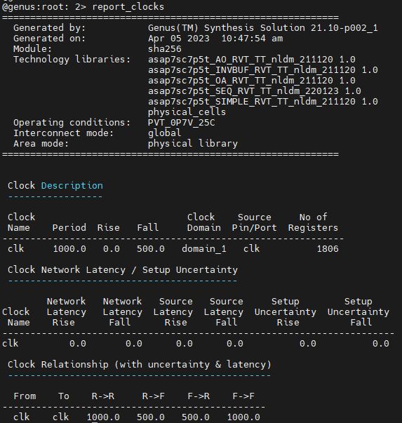
How to read this image: There is a single clock name clk. It's period is 1000ps (1ns), which means a frequency of 1GHz. There is a single clock domain and a total of 1806 registers (flip-flops) are connected to this clock. The duty cycle is 50/50, meaning that the clock is assumed to be a perfect square wave.
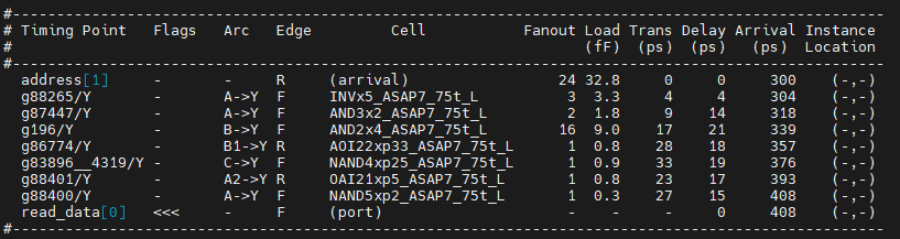
Next, let's have a look at timing. The command we will be using is report_timing. The report looks like this (it may not be a perfect match to your result):
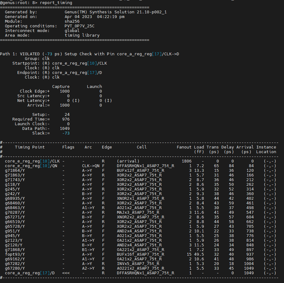
How to read this image: The critical path does not meet the timing constraint. There is a negative slack of 73ps, which means the timed path takes 1073ps to settle, but we only have 1000ps. We can also see where the path starts (core_e_reg_reg[10], clock pin) and where it ends (core_a_reg_reg[17], data pin) -- this is a reg-to-reg path. The report also tells us that the end-point flip-flop has a 24ps setup requirement, meaning that data has to be stable for 24ps for the flip-flop to be able to reliably capture it. This is why in the timing calculation this appears with a negative sign, because we "lose" 24ps for latching. We can also see that the datapath itself takes 1049ps. The individual contribution of each cell that is part of the path is shown as a table. We can also see that most cells are X2, meaning that they are upsized. There are also some outliers that are X12 and X16. All of these are indicators that the synthesis engine worked really hard on this path.
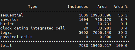
Next, let's have a look at area. There are two commands for that, report_area and report_gates. You can think of the area report as a summary whereas the gates report is more complete. The result looks like this:
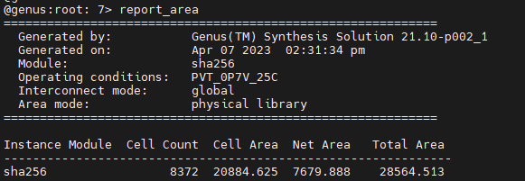
How to read this image: The design has a top-level module named sha256. The design contains 8372 standard cells which occupy 20884 um^2. This is a precise number, obtained by adding the area of each individual cell. Routing all of these cells will incur more area, which Genus estimates at 7679 um^2. This number is not precise since we do not have a layout at this point. The total area is the sum of the two areas. IMPORTANT: in academic papers, both cell area and total area are used and it is not always clear which one is which. It is always good to be clear about what you are reporting.
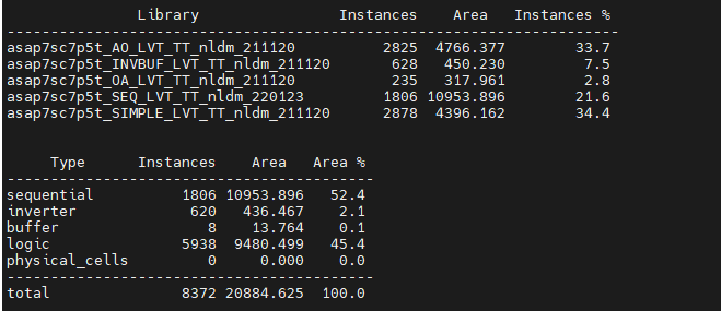
How to read this image: The design uses cells from different libraries. This is not really relevant in this case because the library designers decided to separate their libraries into different files. In practical terms, there is only one standard cell library being used and it is for low Vth (LVT). Next, we see how the area is distributed among different cell types. Not surprisingly, flip-flops account for 52% of the area, which is really typical. Also remember that flip-flops are large cells, often the largest cell in a whole library.
Finally, let's have a look at power. The command we are going to use is report_power. The command output looks like this:
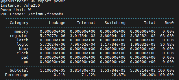
How to read this image: Power consumptions has 3 components: Leakage (or static), Internal, and Switching. Internal and switching are dynamic in nature, meaning that this is power consumed when the circuit is actively computing. In other words, the power consumption here depends on the inputs of the circuit. Internal power is the power consumed by the standard cells themselves. Switching power is related to capacitance charge/discharge of the wires that connect the cells together. Power consumption can come from many components of the circuit, including memories, flip-flops, latches, logic, black boxes, clock distribution, pads, and power management. Because we are not doing physical synthesis, we only have a few of those.
Most of the time we will be interested in checking area, timing, and power reports, so go ahead and remove the comments at the end of script (look for !TODO! markers in the genus.tcl script). This way we will always get the values reported at the end of the synthesis run, any time we run it.
Did you get similar values for area and power? If so, let's move on! Timing should be a mismatch because I created an artificial scenario to show negative timing slack. Your design should have a slack of 0 ps. Is it right?
Now that we have a reference script and we know how to report on the characteristics of a circuit, let's try some more advanced commands and options. The first thing we are going to do is revise our clock specification. We have, so far, defined a clock:
create_clock -name "clk" -period 1000 [get_ports clk]
This is hardly sufficient. It works well for paths that are reg-to-reg since they are bound by clock on the arrival end and on the destination end. But it does not say anything about input-to-reg paths and output-to-reg paths. By default, the tool cannot assume anything about these paths. In the same Genus session from before, we can verify that there is an issue with our inputs with the aid of report_timing. In the terminal, use the following command:
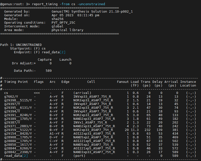
report_timing -from cs
Did it work? It should not have worked because the tool cannot find a constrained path that starts at the "cs" input. It should have said "Some unconstrained paths have not been displayed". There is a workaround to force the tool to time this path by issuing the command report_timing -from cs -unconstrained. The outcome should look like this:
You, the designer, have to tell the tool about the behavior that you want. In most cases, when doing synthesis of a block that is part of a larger chip, all inputs are synchronous to the clock. That means that whatever other logic there is that is generating inputs for your block, it also works on the same clock domain. In order to achieve this behavior, we are going to use the set_input_delay command like this:
set_input_delay -clock clk delay_value [all_inputs]
How to interpret this command: we are telling Genus that all inputs of our design have a relationship with a clock named "clk" and that this relationship has to be respected. This means that every input becomes available (stable) delay_value time units after the clock edge. This amount is discounted from our timing window when doing timing analysis.
There is also an analogous command for the outputs of our block. The command looks like this:
set_output_delay -clock clk delay_value [all_outputs]
How to interpret this command: we are telling Genus that all outputs of our design have a relationship with a clock named "clk" and that this relationship has to be respected. This means that every output must become available (stable) delay_value time units before the next clock edge. This amount is discounted from our timing window when doing timing analysis.
Go ahead and apply these commands to your design in the same Genus session. We are gonna use a value of 300ps for input and output delays. These numbers are a guesstimate because we do not know the environment in which our block will be operating. In a more realistic design, we would have to understand the SoC-related or board-related constraints that apply to the inputs and outputs.
set_input_delay -clock clk 300 [all_inputs]
set_output_delay -clock clk 300 [all_outputs]
When we have our setup right, we can now report timing again and see what we get... Notice that this time we do not need the unconstrained option because the path is now properly constrained.
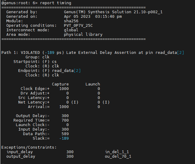
Did you find a timing violation in your design (maybe not exactly the same as in the image)? There should be a violating path that starts from "cs" and ends in "read_data". We are going to fix this in the next task!
In order to fix our timing, we have to apply the input and output delays from the start of the synthesis run. We are going to close Genus, edit our reference script such that it includes the input and output delay constraints, and start Genus again with the same script.
You can check timing after the script is done, there should be no violating paths. Correct?
Now, what happened to our area/power? Because the design is now more constrained, the expectation is that we will have to consume more power and more area to make sure all paths meet timing. Go ahead and check if that is true with the commands report_area and report_power.
Did the area increase? By how much? How about power?
Go ahead and write down the values you obtained in the table. We will need those for comparison later. We also want to collect cell count and area values for comparisons. We will also need to compare the output of report_gates so please save it with the command report gates > gates_from_task_5.rep.
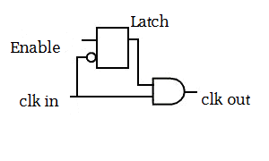
Clock gating is a widely used low-power technique. The idea is that not all flip-flops of your circuit need to toggle at every clock cycle since in many cases they have to hold the same data they were already holding. Synthesis tools are able to automatically infer enable conditions from your source code and created derived clock signals (gated clocks) from it. This is all transparent, the RTL code does not need to be modified by hand to achieve clock gating.
By default, clock gating is not enabled in Genus. To enable it, use the following command:
set_db lp_insert_clock_gating true
So go ahead, modify your synthesis script to include this command and run the entire script again. In order to check if it worked, we can use two different commands:
report_gates or
report_clock_gating
How to read this image: A total of 20 clock gating cells were introduced. A single cell can be shared by many flip-flops. You can check details of how efficient the clock gating procedure was with the
report_clock_gatingcommand.
Now, after clock gating, did the power increase or decrease? By how much? How about timing, was it compromised?
How about area? Did it increase or decrease? This result can be hard to interpret, but it has to do with how clock gating cells are built. Here is the schematic of one of those cells:
What happens is that some enable condition that was potentially part of your critical path can be moved to the clock path. This can be interesting for timing, say now you have one less AND gate in your critical path. Perhaps you do not need to buffer that critical path as much as before and perhaps this can lead to area savings. We can check whether that is true. First, let us generate a new gate report for this design using report gates > gates_from_task_3.rep. Open this report side by side with the previous report from Task 5 and compare them. What happened to the buffers? What happened to the inverters? We can look at the size and number of inverters/buffers to determine how hard did the tool work on optimizing the design. It is not a precise science, but it is good enough for what we are trying to do.
Very often we are interested in finding what is the max frequency of operation of a circuit. The tools cannot give this value directly to you, the process is actually iterative. You have to try one frequency, see if it passes timing, rinse and repeat. You stop doing this when you get a timing slack of 0. However, notice that any design that passes timing, whether it is at 1MHz or at 1GHz, will have a slack of zero. In other words, you have to chase the hardest zero possible.
Just because the process is iterative, it does not mean we have to blindly search for a magical frequency number. You can start with small increments in frequency. Let's say we take our period of 1ns and make it 900ps (1GHz -> 1.11GHz). Will the design still pass timing? Go ahead and modify your synthesis script and try it out.
What happened to area/timing/power/gate count? Write down these values before we move to the next step. You should have noticed an increase in total power but almost no increase in static power. Can you understand why?
Next, we could continue to do small increases in frequency until we converge on a final value. This is a fine approach used quite often and you might need ~5 or so synthesis runs to converge on a final value. But it is not the only approach.
We are going to try something different. We are gonna set a frequency target that is very very high and we are going to expect that the tool will not be able to pass timing. Then we are going to measure by how much we failed to pass timing and subtract that difference from our clock period. This approach is not perfect because the synthesis tools have different behaviors (heuristics) depending on how far from the target they are. In principle, setting an impossible target may lead the tool to not optimize it very well since it knows it will never get near the target. With this disclaimer in mind, let's set the clock period to 500ps and see what happens. For that, we are going to use the command create_clock -name "clk" -period 500 [get_ports clk]. Change that line in your script and fire away. Because the target is very hard, the execution time will increase considerably.
After a few minutes, you should get a result like this from report timing:
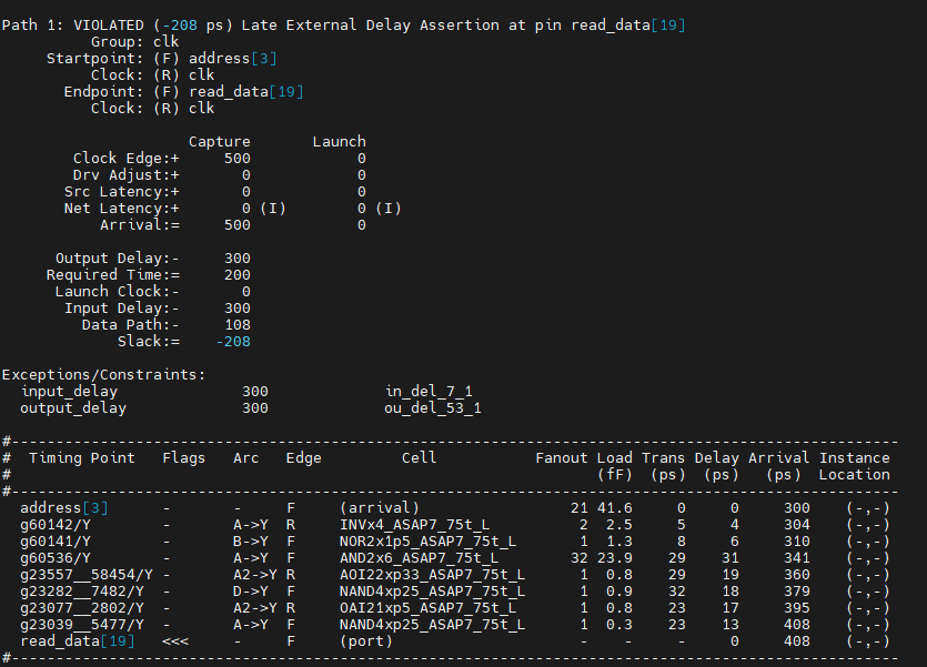
It looks like we overshot our target by 208ps (your results may be slightly different depending on tool version).
What we can do next is go back to our synthesis script, change the period to 500+208=708ps and start the process again. This should be a fairly good approximation of the max frequency we can operate this design at, give or take a few picoseconds.
Let's take note again of the design characteristics at 500ps and at 708ps clock periods. Write down the area/timing/power/gate count that you obtained from the runs (even if this circuit does not respect our constraints, the data is interesting for comparison).
Genus supports multiple effort levels in its many internal engines. The idea is that you can ask the tool to work harder on the problem and this will incur a penalty in execution time. By default, most effort-related variables are set to medium. Since we are doing a relatively small design, selecting high effort is a no brainer. So go ahead and increase the effort by setting the following variables in your script:
set_db syn_generic_effort high
set_db syn_map_effort high
set_db syn_opt_effort extreme
How to interpret these commands: syn_generic is the first part of the synthesis process and controls how the provided RTL is transformed into a graph for further processing. It also controls how arithmetic operators (+ - / * %) are identified and instantiated in your design. syn_map is the process of transforming the generic graph representation of the design into a set of interconnected standard cells. Thus the name mapping. syn_opt starts the optimization engine of Genus. It has a long list of tricks that it attempts to apply to the design in order to improve timing and reduce area/power. Most of these are proprietary and there is very little you can infer from the logs. Just trust the tool, it will optimize a lot.
Run your script again with these new settings and take note of your results. Did something change?
Next, we are going to increase the effort using different commands that control power-related optimizations. Set the following variables in your script:
set_db lp_power_analysis_effort high
set_db power_optimization_effort high
set_db design_power_effort high
How to interpret these commands: lp_power_analysis_effort, power_optimization_effort, and design_power_effort are interrelated. They control how much time and effort should the tool spend on power-related optimizations.
Now run your synthesis script again. You have to close Genus and start from scratch, these settings do not work well if applied after the design has already been synthesized. What happened to your design? Is it more efficient? Go ahead and annotate the area/timing/power/cell count values that you got.
Let us assume our design has a very low frequency of operation, something in the range of 1MHz. This is representative of a very constrained environment, perhaps in a passive RFID tag. What happens if you synthesize the design and target 1MHz as frequency? Think about it before you do. What do you expect will happen to area/power/timing/cell count? How about the balance/ratio between dynamic power vs. static power?
Run the synthesis script again, but with the aforementioned 1MHz clock (1000000ps period). Collect results and compare. Did you notice how much the contribution of the static power went up? (from less than 1% to more than 85%!)
What can you do to save more static power if your design is really constrained? Not much. By default, Genus optimizes for static instead of dynamic power. Only RTL changes would help further. Or changing the standard cell library...
In our reference script, we are making use of LVT cells. Meaning that these cells have a low voltage threshold and swing faster from 1->0 and 0->1. In most cases, libraries will offer two other cell variants: RVT and HVT.
LVT cells have a low voltage threshold and for this reason switch faster and consume more power. HVT cells have a higher voltage threshold and switch slower, but at a reduced power. RVT cells have are a middleground between the two. RVT cells are also called SVT, S=Standard, R=Regular.
The standard cell library we are working with has 3 different Vt levels: regular, low, super low. If our target circuit is really intended to run at 1MHz and we have a slack of thousands of picosends, we can safely switch to an RVT library to save even more power. So let's go ahead and edit our reference script to use only RVT cells. Then run synthesis again for the same 1MHz target. Collect area/power/timing/cell count values and compare with the previous run.
Are you saving power by using RVT cells? How much? Write down all the design characteristics after you switched to RVT cells.
In general, we provide the synthesis tools with all flavors of standard cells available in a library and let the tools mix and match. For critical paths, the tool will prefer LVT cells (faster and power hungry). For slow paths, the tool will prefer HVT cells (slower but power efficient).
Execute synthesis again with a target of 708ps, but now consider all three VTs. Take note of the results and add them to your tables.
In some really specific cases, we might want to tell the synthesis tool not to use a few standard cells. For instance, some cells might be really hard to route and are giving us a headache in physical synthesis. We can go ahead and tell the tool set_dont_use problematic_cell. In another scenario, we might have developed specific cells of our own and we want to prevent the tool from using the regular ones available in the library. This usually causes a small penalty. So let's evaluate this penalty.
Then, we are going to prevent Genus from using the cell named AOI22xp33_ASAP7_75t_L. This cell is notoriously hard to route because it is very small and contains many inputs. Therefore, it has a high pin density that creates local routing problems. To prevent Genus from using it, we are going to issue the command set_dont_use AOI22xp33_ASAP7_75t_L true. Then we are going to run our synthesis script again.
What happened to cell count/area/power/timing? Make comparisons and write the values down.
Let us say we are not happy with the results of our synthesis so far. What other tricks can we employ to get better results? The options are limited at this point, but we can try a few things...
Genus has an incremental mode to syn_opt that can be issued with the command syn_opt -incremental. This works as an optimization on top of an optimization. It can be called many times and sometimes it is able to get a few picoseconds of improvement in timing. Run the script again, but this time add this command right after syn_opt. Write down the results that you obtained for area/power/timing/cell count and compare with the previous run.
What changed?
Before moving on, do a report_timing on the further optimized design. Check where the critical path, where it starts and where it ends.
Retiming is the process of rebalancing the logic of your design so a higher clock frequency can be achieved. The figure is rather self-explanatory: flip-flops are TIMING barriers and the logic can be freely moved with respect to them. The only consequence of this approach is that the design becomes harder to validate/simulate. A flip-flop that used to hold an intermediate result at cycle X now may not hold it at any given clock cycle. There are also new flip-flops added to the design that do not have any equivalents in the original design.
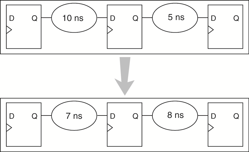
Given the image below and the general concept of how pipelining works, do you think we can apply it to our design? Think about the critical path you determined in the previous step. Is pipelining useful in that scenario?
The SHA256 core we are working with has in2out paths that are not flopped. This is generally considered a bad practice and it is particularly bad when we have strict input delay and output delay constraints. We are going to go ahead and fix this "problem" by adding a pipeline stage to the output of our SHA256 module. Notice that this will increase the latency by 1 additional clock cycle. The new code will loke like this (open sha256_pipe.v in a text editor and inspect):
Now are going to go ahead and synthesize this new code. We are going to change our list of input files to point to sha256_pipe.v instead of sha256.v. All other files remain unchanged. You should proceed with our current synthesis script (708ps clock period and with the incremental opt). We are going to do retiming just yet. What happened? Is the circuit faster, slower, bigger, smaller, power hungry? How many additional flip-flops are there? Could you have predicted the increase in flip-flop count? What happened to the critical path? Write down all the design characteristics before moving on.
Now our design is so freaking good we are going to go wild on the clock frequency. Let's aim for > 2.22GHz (period = 450ps) and see what happens. Start your Genus run again with a modified script for this aggressive clock target. Did it pass timing? What happened to area/power/gate count? Write those values down.
Finally, we are going to apply our very last trick to try to meet timing. We are going to try to retime this design. Start your synthesis again with retiming enabled. What happened? Write it down!
When a design fails timing, it is important to have a look at where it fails (critical path) but also how often it fails. WNS stands for worst negative slack and it is related to the single most critical path. TNS stands for total negative slack and is the sum of the negative slacks of all paths that fail timing checks. If your TNS value is very close to your WNS, this means there is only one or a few paths that are the culprits -- you should probably work on them. If TNS is many times higher than WNS, this means that the problem is more widespread and fixing one single path will just push the problem to another place. From the Genus logs, can you find the WNS and TNS values? They are printed on the screen repeatedly during optimizations.
There are several warnings issued by Genus that are quite benign and relate to how the standard cell library has been described. These warnings can be supressed if you want to by using the command supress_messages {MSG_CODEi MSG_CODEj}.
There is very little benefit in using Genus GUI. One interesting feature is a timing histogram that is otherwise hard to get from the terminal interface. To start the GUI, issue the command gui_show. Once the GUI loads, on the main menu, click on Timing->Debug Timing. Click OK on the popup, don't change anything. You will get a screen like this:
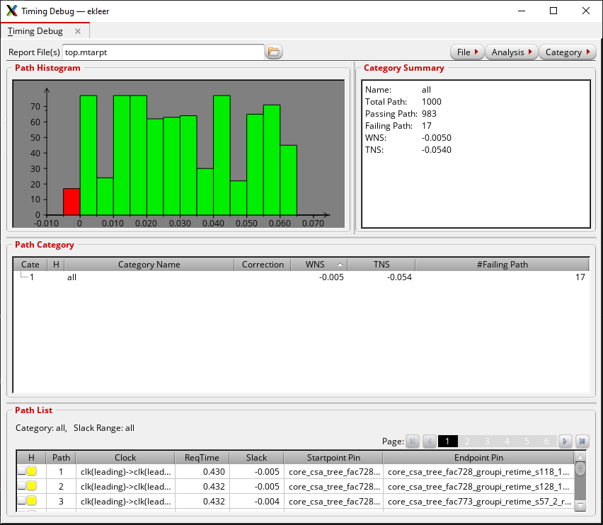
The number of failing paths is generally small, there are only 17 of them. You can inspect these paths one by one and you will see there is a pattern in their starting point. This is indication of what portion of the design could be a candidate for improvement.
An experienced designer can look at this sort of plot and understand if they are leaving too much on the table or if the design is just about right.
Naturally, after logic synthesis comes physical synthesis. The amount of user-guided effort is generally higher in that stage, there is a lot to talk about. Here is a good related repo that uses the same 7nm ASAP library: https://github.com/Centre-for-Hardware-Security/asap7_reference_design